Connector orientation errors on PCBAs occupy a special category in the field return data that electronics manufacturers track. Unlike solder defects or missing components — which are often caught by functional test before shipping — a wrong-orientation connector frequently passes functional test at the board level, makes it into an assembled product, and then causes a failure in the field when the mating harness is connected with force and the wrong-keyed connector damages the header or back-feeds voltage to the wrong pin. The cost signature is distinctly worse than typical manufacturing defects: it's a field return, not a production line rework.
The vision inspection problem for connector orientation is also qualitatively different from the surface defect detection we typically talk about on stamping or machined part lines. Orientation detection is a classification problem with a defined correct answer — the connector either faces the right direction or it doesn't. Surface defect detection is an anomaly detection problem — you're looking for anything that deviates from the clean surface baseline. The training strategy, the model architecture, and the imaging requirements differ meaningfully between them.
Why connector orientation errors occur and persist
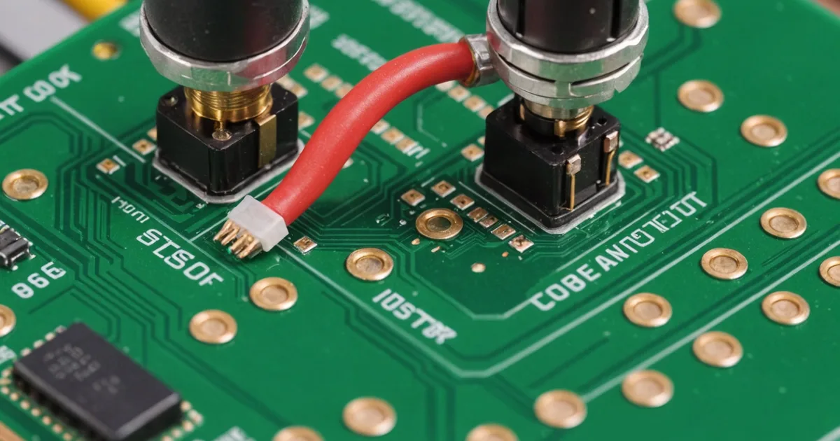
Most PCB connectors that are susceptible to orientation errors are through-hole or hand-placed SMD components where the placement direction is determined by the operator. Polarized JST, Molex MicroFit, and dual-row pin headers are the most common categories. The connector housings are designed with polarity keys — raised ribs, asymmetric key features, a beveled corner — that are meant to prevent mis-insertion into the mating connector. But when the connector is being placed into a PCB footprint (not mated to another connector), there is no mechanical prevention of wrong-orientation placement. The through-hole pins fit in the holes regardless of which end is at pin 1.
The orientation indicator on the connector housing — typically a small triangle, a notch, or a colored stripe — is visually subtle. At volume, operators rotate between board types and component feeders. The error rate for connector orientation on hand-placement lines is typically in the range of 1–5 per 1,000 boards, which sounds small but is significant at high volumes: a line producing 200 boards per shift can have 1–10 orientation errors per shift, and each one is a potential field return rather than a caught-and-reworked defect.
How orientation detection differs from surface defect detection as an ML problem
The core difference is in what the model needs to learn. Surface defect detection requires the model to learn the visual signature of deviations from a normal clean surface — by definition, a discriminative task against an "everything else" background. The defect class is defined by what it is, and the negative class is the normal surface.
Orientation detection requires the model to learn two explicit classes: correct orientation and incorrect orientation. Both classes look like a properly placed connector — the same component, the same solder joints, the same color housing. The distinction is the direction of the polarity indicator, the position of the key feature, or the orientation of the contact pin row relative to a reference on the board.
This means that the feature the model uses to distinguish the two classes is local — a specific small region of the connector housing — rather than global. A model trained on full-board images tends to give too much attention to surrounding components and board features and too little to the polarity indicator itself. We train orientation models with tight crops around the connector region, at a pixel density that clearly resolves the orientation key feature, as separate classification heads rather than as part of a general board-level inspection model.
Imaging requirements for orientation keys
The critical imaging constraint is resolution at the polarity indicator. For a JST PH 2mm connector, the polarity notch on the housing is approximately 1mm wide. To reliably classify orientation from the notch position, you need at least 5–8 pixels across the notch width — that's a pixel pitch of under 0.2mm/pixel at the sensor, which typically requires a macro lens or a short working distance on a standard C-mount industrial lens.
For board-level inspection with multiple connectors at different positions, this creates a field-of-view vs. resolution tradeoff. You can't inspect a full board at the resolution required for orientation keys with a single camera from a workable working distance. The practical solutions are:
Multiple cameras, each covering a subregion at adequate resolution. This is the common approach on dedicated PCBA AOI lines where capital equipment cost is acceptable.
Sequential frame capture at multiple positions using a movable camera head or a board transport with multiple inspection stations. More latency, but achievable with a single camera on lines where throughput allows it.
ROI-focused inference: capture the full board image at lower resolution, use a first-stage detection model to locate each connector, then crop and upsample the connector ROI for the orientation classification model. This works when the connector location is approximately known and consistent, which is typically true for wave-soldered through-hole boards but may not be reliable for hand-placement variation.
Training data considerations specific to orientation detection
Unlike surface defect training — where wrong-orientation examples are rare by definition because defects are rare — orientation training data is easier to generate deliberately. Wrong-orientation examples can be intentionally assembled by a technician: place 50 boards with connectors correctly oriented, then place 50 boards with the target connector type in the wrong orientation. This is a controlled process, not dependent on collecting rare production failures.
The challenge is getting representative variation within each orientation class. A correctly oriented connector can vary in the z-axis height (insertion depth variation), in x-y registration (hand placement ±0.5–1mm), and in illumination (depending on the positioning of adjacent components that shadow the connector housing). Training examples should cover this intra-class variation — otherwise the model will flag in-tolerance placement variation as orientation errors, producing false positives on the variation you see from normal hand placement.
Augmentation for orientation detection is more constrained than for surface defects. You must not use rotation augmentation beyond ±5–10 degrees, because the orientation labels themselves encode rotation information — an image rotated 90 degrees with a correct-orientation label is now a mislabeled training example. Spatial augmentation should be limited to translation (±10% of the ROI width), mild shear, and scale (±5%). Aggressive color augmentation should be avoided for the same reasons as surface defect training: the polarity indicator's color contrast relative to the housing is a valid feature.
The production integration: reporting vs. rejecting
Orientation error detection has a different production integration story than surface defect detection. A false positive on a surface defect means an acceptable part went into the reject bin — recoverable. A false positive on orientation detection means a good board was pulled from the line, inspected by a technician, confirmed correct, and returned. That's labor cost, but no material loss.
More importantly: orientation errors on PCBAs are generally reworkable. A wrong-orientation connector can be desoldered, reorientated, and resoldered. This is a rework event, not scrap. The economics of false positives look different: each false positive costs rework time (10–15 minutes per board for through-hole connector rework), but a false negative costs a field return (which is typically 50–100× the rework cost by the time the return logistics, failure analysis, and customer communication are factored in).
This asymmetry argues for setting the orientation model threshold lower — accepting more false positives (rework events) to prevent false negatives (field returns). The exact threshold calibration depends on the cost ratio for your specific product, but for most electronics assemblies going to end-customer products, the asymmetry is large enough that a 0.5% FP rate is entirely acceptable for orientation detection in a way that it might not be for surface defect detection on a commodity stamping line.
The integration for orientation detection is typically a rework station flag rather than an automated hard reject: a visual alert at the operator station and a database record, rather than a physical actuator rejecting the board. The volume of orientation errors is too low (and the rework value too high) to justify automated physical handling at most PCBA production rates.